- 您现在的位置:买卖IC网 > Sheet目录325 > FAN73833MX (Fairchild Semiconductor)IC HALF BRIDGE GATE DRIVER 8-SOP
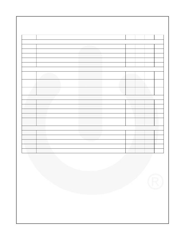
Electrical Characteristics
V BIAS (V DD , V BS ) = 15.0 V, and ? T A =25 ? C, unless otherwise specified. The V IN and I IN parameters are referenced to
COM. The V O and I O parameters are referenced to V S and COM and are applicable to respective outputs HO and LO.
Symbol
Parameter
Condition
Min.
Typ.
Max.
Unit
SUPPLY CURRENT SECTION
I QBS
I QDD
I PBS
I PDD
I LK
Quiescent V BS supply current
Quiescent V DD supply current
Operating V BS supply current
Operating V DD supply current
Offset supply leakage current
V IN =0 V or 5 V
V IN =0 V or 5 V
f IN =20 kHz, rms value
f IN =20 kHz, rms value
V B =V S =600 V
35
80
420
420
100
200
750
750
10
μA
μA
μA
μA
μA
POWER SUPPLY SECTION
V DDUV+
V BSUV+
V DDUV-
V BSUV-
V DDUVH
V BSUVH
V DD and V BS supply under-voltage ?
positive going threshold
V DD and V BS supply under-voltage ?
negative going threshold
V DD supply under-voltage lockout ?
hysteresis
8.2
7.2
9.2
8.3
0.9
10.1
9.2
V
V
V
GATE DRIVER OUTPUT SECTION
V OH
V OL
High-level output voltage, V BIAS -V O
Low-level output voltage, V O
I O =20 mA
1.0
0.6
V
V
I O+(4)
I O-(4)
V S
Output high short-circuit pulse current
Output low short-circuit pulsed current
Allowable negative V S pin voltage for
IN signal propagation to HO
V O =0 V, V IN =5 V with PW<10 μs
V O =15 V, V IN =0 V with PW<10 μs
250
500
350
650
-9.8
-7.0
mA
mA
V
LOGIC INPUT SECTION (INPUT and SHUTDOWN)
V IH
V IL
Logic "1" input voltage
Logic "0" input voltage
2.5
1.2
V
V
I IN+
I IN-
R PD
Logic "1" input bias current
Logic "0" input bias current
Input pull-down resistance
V IN =5 V
V IN =0 V
50
100
100
2.0
μA
μA
K ?
Note:
4. This parameter is guaranteed by design.
? 2008 Fairchild Semiconductor Corporation
FAN73833 ? Rev.1.0.2
5
www.fairchildsemi.com
发布紧急采购,3分钟左右您将得到回复。
相关PDF资料
FAN7383MX
IC GATE DVR HALF BRIDGE 14-SOIC
FAN7384MX
IC DRIVER GATE HALF BRIDGE 14SOP
FAN7385MX
IC GATE DRIVER HISIDE 2CH 14-SOP
FAN7388MX
IC GATE DRIVER HALF BRIDG 20SOIC
FAN73892MX
IC GATE DVR HALF BRDG 3PH 28SOIC
FAN7389MX
IC GATE-DRIVE 3PH HALFBRDG 24SOP
FAN73901M
IC GATE DRIVER HI/LOW SIDE 8SOIC
FAN7390M1X
IC DRIVER GATE HI/LO SIDE 14-SOP
相关代理商/技术参数
FAN7383M
功能描述:功率驱动器IC Half Brige Gate RoHS:否 制造商:Micrel 产品:MOSFET Gate Drivers 类型:Low Cost High or Low Side MOSFET Driver 上升时间: 下降时间: 电源电压-最大:30 V 电源电压-最小:2.75 V 电源电流: 最大功率耗散: 最大工作温度:+ 85 C 安装风格:SMD/SMT 封装 / 箱体:SOIC-8 封装:Tube
FAN7383MX
功能描述:功率驱动器IC Half Bridge Gate Driver RoHS:否 制造商:Micrel 产品:MOSFET Gate Drivers 类型:Low Cost High or Low Side MOSFET Driver 上升时间: 下降时间: 电源电压-最大:30 V 电源电压-最小:2.75 V 电源电流: 最大功率耗散: 最大工作温度:+ 85 C 安装风格:SMD/SMT 封装 / 箱体:SOIC-8 封装:Tube
FAN7383MX_WS
功能描述:功率驱动器IC MOS DRVR 600V 0.65A 4-Out Hi/Lo RoHS:否 制造商:Micrel 产品:MOSFET Gate Drivers 类型:Low Cost High or Low Side MOSFET Driver 上升时间: 下降时间: 电源电压-最大:30 V 电源电压-最小:2.75 V 电源电流: 最大功率耗散: 最大工作温度:+ 85 C 安装风格:SMD/SMT 封装 / 箱体:SOIC-8 封装:Tube
FAN7384
制造商:FAIRCHILD 制造商全称:Fairchild Semiconductor 功能描述:Half-Bridge Gate-Drive IC
FAN7384_0702
制造商:FAIRCHILD 制造商全称:Fairchild Semiconductor 功能描述:Half-Bridge Gate-Drive IC
FAN7384_09
制造商:FAIRCHILD 制造商全称:Fairchild Semiconductor 功能描述:Half-Bridge Gate-Drive IC
FAN7384M
功能描述:功率驱动器IC Half Bridge Gate Driver RoHS:否 制造商:Micrel 产品:MOSFET Gate Drivers 类型:Low Cost High or Low Side MOSFET Driver 上升时间: 下降时间: 电源电压-最大:30 V 电源电压-最小:2.75 V 电源电流: 最大功率耗散: 最大工作温度:+ 85 C 安装风格:SMD/SMT 封装 / 箱体:SOIC-8 封装:Tube
FAN7384MX
功能描述:功率驱动器IC Half Bridge Gate RoHS:否 制造商:Micrel 产品:MOSFET Gate Drivers 类型:Low Cost High or Low Side MOSFET Driver 上升时间: 下降时间: 电源电压-最大:30 V 电源电压-最小:2.75 V 电源电流: 最大功率耗散: 最大工作温度:+ 85 C 安装风格:SMD/SMT 封装 / 箱体:SOIC-8 封装:Tube
